


 275 / 308

275
Materials Science and Mechanics of Materials
Crystal Plasticity in the Field of Microelectronics
Growing demands on performance and durability of
integrated circuits require an understanding of possible
failure mechanisms like crack initiation within the interlayer
dielectric (ILD) and surface roughening of the metalliza-
tion plate. One main cause for these phenomena arises
from the mismatch in thermal expansion between the
materials involved (conductor paths and metallization
plate are made of aluminum and the surrounding ILD of
silicon oxide) leading to thermo-mechanical loads and,
consequently, to various types of damage. Throughout
their life, the electronic components undergo millions of
load cycles, so that an experimental life cycle analysis
during the development process is costly and may not be
feasible.
In cooperation with the Max-Planck-Institut für Eisen
forschung, a crystal plasticity material model was
developed which takes into account microstructure, grain
orientation, grain size and thermal expansion behavior of
the metallic components involved and the temperature
dependency of the constitutive material parameters.
Currently, a comprehensive review of this material model
named DAMASK is being prepared for publication. There,
one of the examples shows the utilization of crystal plas-
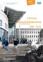
ticity in the field of microelectronics. In this study the influ-
ence of the microstructure of the conductor paths on the
probability of crack initiation is investigated. Since brittle
failure occurs within the ILD, the maximum principal stress
Simulation model representing a part of an integrated circuit at the end of a
heating cycle. The two cross sections show a vector representation of the
maximum principal stress within the ILD. (Source: WKM)
is considered as a measure to quantify the likelihood of
the occurrence of brittle failure. The texture of aluminum
components affects the stress level within the ILD as well
as within the conductor paths. The investigations suggest
that randomizing the predominant texture which arises
from the manufacturing process increases the lifetime of
the microelectronic component.
High Entropy Alloys
High entropy alloys (HEA) represent a new approach in
materials design.
Initially, HEAs were defined by their equiatomic or near
equiatomic composition. At least five different elements
take a random arrangement in the crystal lattice. This
leads to extreme lattice distortion, which results in a great
resistance against plastic deformation and a sluggish lat-
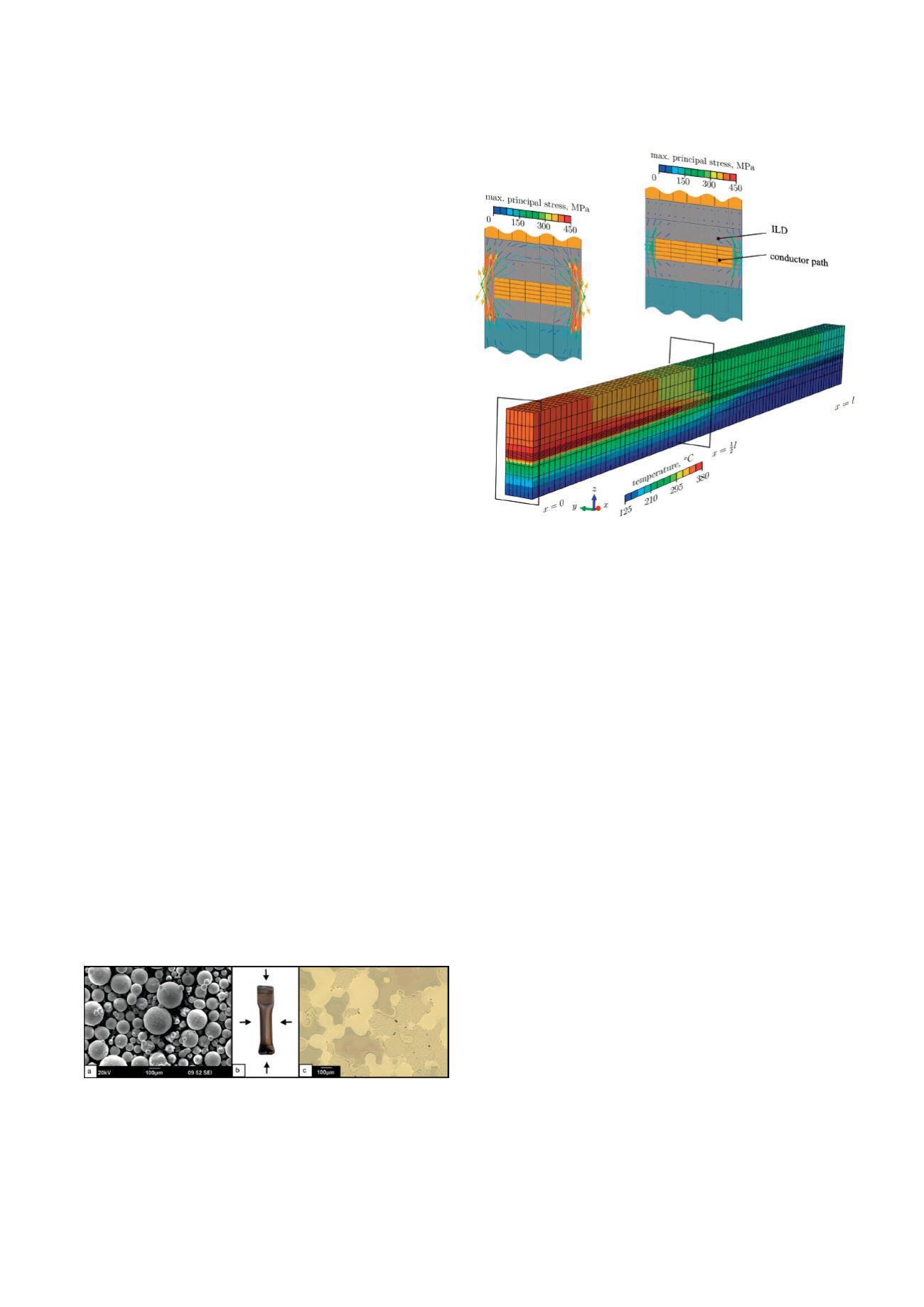
Mixing of metal powders to a HEA concentration (a). Densification of pow-
der via encapsulation and hot isostatic pressing (b). Densified material with
diffusion zones between the original powder particles (c). (Source: WKM)
tice diffusion even at high temperatures. Previous studies
on HEA showed that also non-equiatomic compositions
form a random solid solution and reach HEA-characteristic
material properties. Due to this, the strict definition of HEA
has been relaxed and additional material compositions
were declared as HEA. A promising research approach is
the production of HEA based on conventional alloys. The
aim is to effectively combine outstanding properties and
process technologies of existing material systems with the
advantages of HEA compositions.
At WKM, conventional powder alloys and elemental
powders are combined with the aim of achieving HEA
compositions. For this purpose, powder mixtures are
encapsulated and compressed via hot isostatic pressing.
Microstructural analysis of the solid materials produced
is performed via light microscopy, scanning electron
microscopy as well as EDX and XRD methods. Mechanical